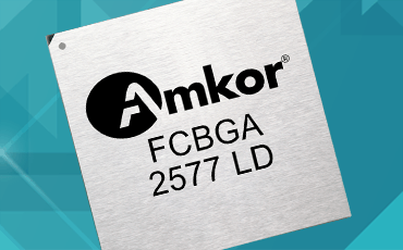
Improve electrical performance and incorporate higher IC functionality
Amkor Flip Chip BGA (FCBGA) packages are assembled around state‑of‑the‑art, single unit laminate or ceramic substrates. Utilizing multiple high density routing layers, laser drilled blind, buried and stacked vias, and ultra fine line/space metallization, FCBGA substrates have the highest routing density available. By combining flip chip interconnect with ultra advanced substrate technology, FCBGA packages can be electrically tuned for maximum electrical performance. Once the electrical function is defined, the design flexibility enabled by flip chip also allows for significant options in final package design. Amkor offers FCBGA packaging in a variety of product formats to fit a wide range of end application requirements.

Technology Solutions
- Substrates
- 4-18 layer laminate build-up substrates
- High CTE ceramic
- Coreless
- Bump Types
- Eutectic Sn/Pb
- Pb-free (green)
- Cu pillar(array and fine pitch peripheral)
- Package Formats
- Bare die
- Lidded
Features
- Die sizes up to 31 mm
- Package sizes from 10 mm to 67.5 mm (85 mm in development)
- 0.4 mm, 0.5 mm, 0.65 mm, 0.8 mm and 1.0 mm pitch BGA footprints
- 90 µm minimum array bump pitch
- <90 µm minimum peripheral bump pitch
Additional Package Options
- Wafer Node ≥7 nm qualified, 5 nm in qualification
- SMT components on top or bottom side
- Multi-die capability
- Memory components on top side
- Variety lid material options
- Grounded lid
- Custom BGA footprints
Questions?
接触一个Amkor expert by clicking the request info button below.
